NEET Physics · Class 12 · 49 questions · 2014 to 2026

NEET Semiconductor Electronics previous year questions

49 questions on Semiconductor Electronics from 18 NEET and AIPMT papers, 2014 to 2026, newest first; on average 2.7 a paper. Open a question for NTA's official answer.

Answers are NTA's official final key, shown for NEET 2021, NEET 2022, NEET 2023, NEET 2023 (Manipur), NEET 2025 and NEET 2026 Re-Examination (21 June). The other papers are given without answers until NTA's key for them is in hand; we do not put an answer of our own in its place. The questions are from published copies of each paper, not from NTA's own booklets, so a word here and there may differ from the printed paper. Chapter-wise weightage

NEET 2026 Re-Examination (21 June) (2)NEET 2026 (3 May) (3)NEET 2025 (2)NEET 2024 (4)NEET 2023 (Manipur) (4)NEET 2023 (3)NEET 2022 (3)NEET 2021 (3)NEET 2020 (3)NEET 2019 (Odisha) (2)NEET 2019 (2)NEET 2018 (3)NEET 2017 (3)NEET 2016 Phase II (3)NEET 2016 Phase I (3)AIPMT 2015 Re-Test (2)AIPMT 2015 (2)AIPMT 2014 (2)
NEET 2026 Re-Examination (21 June)

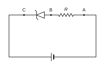
NEET 2026 Re-Examination (21 June) · Q8 · Voltage across a reverse-biased Zener diode circuit
An ideal Zener diode with breakdown voltage of – 3 V is reverse biased with a negative input voltage Vi = – 5 V. The magnitude of voltage difference between points B and A is:
A rectangular loop: on the top wire, from left to right, point C, a Zener diode whose arrow points towards C, point B, a resistor R and point A; a cell on the bottom wire with its long plate on the left.
NTA's answer

Answer: (3) 2 V

From NTA's final answer key for NEET 2026 Re-Examination (21 June).
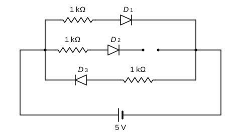
NEET 2026 Re-Examination (21 June) · Q28 · Comparing depletion widths of three diodes across a battery
Three identical p-n junction diodes D1, D2 and D3 are connected across a battery as shown in the figure. If the width of the depletion regions of D1, D2 and D3 are W1, W2 and W3, respectively, then the correct option is:
Three branches between a left and a right vertical rail. Top: a 1 kΩ resistor then diode D1 pointing right. Middle: a 1 kΩ resistor, diode D2 pointing right, then an open gap between two dots before the right rail. Bottom: diode D3 pointing left, then a 1 kΩ resistor. A 5 V cell, long plate on the left, is connected by an outer loop to the two rails at the level of the middle branch.
NTA's answer

Answer: (4) W3 > W2 > W1

From NTA's final answer key for NEET 2026 Re-Examination (21 June).

NEET 2026 (3 May)
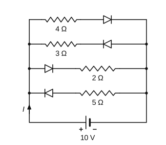
NEET 2026 (3 May) · Q3 · Current in a circuit containing ideal diodes
The current I in the circuit shown below is: (All diodes are ideal and identical)
Four branches in parallel between a left and a right rail: (top) 4 Ω then a diode pointing right; 3 Ω then a diode pointing left; a diode pointing right then 2 Ω; a diode pointing left then 5 Ω. A 10 V cell joins the bottoms of the rails, + on the left; current I marked upward on the left rail just above the cell.
Answer

NTA's official answer key for NEET 2026 (3 May) is not in hand yet. This page will carry the answer when it is; we do not put an answer of our own in its place.
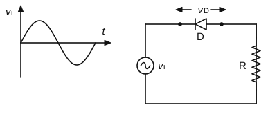
NEET 2026 (3 May) · Q24 · Waveform of the voltage across a diode in a circuit
In the circuit shown below, the voltage appearing across the diode D will be of the form:
Left, a graph of input vi against t: one sine cycle, positive half first. Right, a loop with an ac source vi on the left side, a diode D on the top wire pointing left (conducting right to left) with vD marked across it, and a resistor R on the right side. Options are vD–t graphs: (1) two positive half-sine humps; (2) one positive hump, then zero; (3) two negative half-sine troughs; (4) one full sine cycle, positive half first.
Answer

NTA's official answer key for NEET 2026 (3 May) is not in hand yet. This page will carry the answer when it is; we do not put an answer of our own in its place.

NEET 2026 (3 May) · Q44 · Statements on forward-bias current of a p-n junction diode
Two statements are given below:
I. When the forward bias voltage across a p-n junction diode increases above a certain threshold voltage, the diode current increases significantly.
II. This current is called reverse saturation current.
Choose the CORRECT answer from the options given below:
Answer

NTA's official answer key for NEET 2026 (3 May) is not in hand yet. This page will carry the answer when it is; we do not put an answer of our own in its place.

NEET 2025
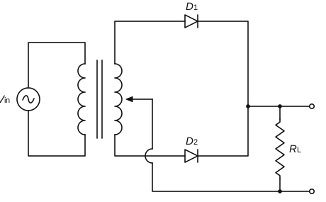
NEET 2025 · Q15 · Bias states of the two diodes in a full wave rectifier at a given instant
A full wave rectifier circuit with diodes (D1) and (D2) is shown in the figure. If input supply voltage Vin = 220sin(100πt) volt, then at t = 15 msec
Centre-tap full-wave rectifier: an ac source Vin across the primary coil of a transformer with an iron core; the top end of the secondary goes through diode D1 and the bottom end through diode D2, both pointing right, to a common wire that feeds the top of load resistor RL and the upper output terminal; the centre tap of the secondary is wired, hopping over the D2 lead, to the bottom of RL and the lower output terminal.
NTA's answer

Answer: (3) or (4)

From NTA's final answer key for NEET 2025; the key accepts either option.
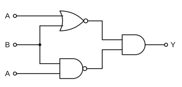
NEET 2025 · Q25 · Gate equivalent to a given logic implementation
The output (Y) of the given logic implementation is similar to the output of an/a ______ gate.
Logic circuit with inputs A (top), B (middle) and A (bottom): A and B feed a NOR gate; B and the lower A feed a NAND gate; the two outputs feed an AND gate whose output is Y.
NTA's answer

Answer: (2) NOR

From NTA's final answer key for NEET 2025.

NEET 2024
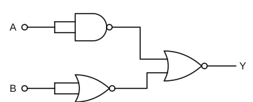
NEET 2024 · Q6 · Gate equivalent to a given logic gate circuit
The output (Y) of the given logic gate is similar to the output of an/a:
Input A feeds both inputs of a NAND gate and input B feeds both inputs of a NOR gate; the two gate outputs are the inputs of a final NOR gate whose output is Y.
Answer

NTA's official answer key for NEET 2024 is not in hand yet. This page will carry the answer when it is; we do not put an answer of our own in its place.

NEET 2024 · Q7 · Statements on solar cell characteristics and reverse-bias current
Consider the following statements P and Q and identify the correct answer:

P. For a solar-cell, the I-V characteristics lies in the IV quadrant of the given graph.
Q. In a reverse biased pn junction diode, the current measured in (μA), is due to majority charge carriers.
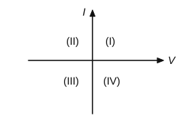
Current I on the vertical axis and voltage V on the horizontal axis crossing at the centre; the quadrants are labelled (I) upper right, (II) upper left, (III) lower left and (IV) lower right.
Answer

NTA's official answer key for NEET 2024 is not in hand yet. This page will carry the answer when it is; we do not put an answer of our own in its place.

NEET 2024 · Q21 · Boolean expression for a given truth table
A logic circuit provides the output Y as per the following truth table:
ABY
001
010
101
110
The expression for the output Y is:
Answer

NTA's official answer key for NEET 2024 is not in hand yet. This page will carry the answer when it is; we do not put an answer of our own in its place.

NEET 2024 · Q36 · Circuit in which a bridge with a diode in one arm can balance
Choose the correct circuit which can achieve the bridge balance.
Answer

NTA's official answer key for NEET 2024 is not in hand yet. This page will carry the answer when it is; we do not put an answer of our own in its place.

NEET 2023 (Manipur)

NEET 2023 (Manipur) · Q2 · Material with the smallest resistivity among conductors, semiconductors and insulators
On the basis of electrical conductivity, which one of the following material has the smallest resistivity?
NTA's answer

Answer: (4) Silver

From NTA's final answer key for NEET 2023 (Manipur).
NEET 2023 (Manipur) · Q11 · Dopant that makes germanium a p-type semiconductor
A p-type extrinsic semiconductor is obtained when Germanium is doped with:
NTA's answer

Answer: (2) Boron

From NTA's final answer key for NEET 2023 (Manipur).

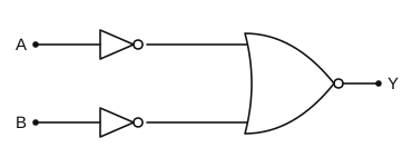
NEET 2023 (Manipur) · Q16 · Single gate equivalent to a circuit of NOT and NOR gates
The given circuit is equivalent to:
Logic circuit: input A passes through a NOT gate and input B through another NOT gate; the two outputs feed a NOR gate (OR shape with an output bubble) whose output is Y. Options, each with inputs A, B and output Y: (1) an OR gate; (2) an AND gate; (3) a NOR gate; (4) a NAND gate.
NTA's answer

Answer: (2)

From NTA's final answer key for NEET 2023 (Manipur).

NEET 2023 (Manipur) · Q17 · Statements on a transistor's structure and biasing

The above figure shows the circuit symbol of a transistor. Select the correct statements given below:
i. The transistor has two segments of p-type semiconductor separated by a segment of n-type semiconductor.
ii. The emitter is of moderate size and heavily doped.
iii. The central segment is thin and lightly doped.
iv. The emitter base junction is reverse biased in common emitter amplifier circuit.
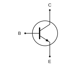
Transistor circuit symbol inside a circle: base lead B from the left to a vertical bar; collector C leaves the bar upwards to the top; emitter E leaves the bar downwards to the bottom, with the arrow on the emitter pointing away from the base, towards E.
NTA's answer

Answer: (2) ii and iii

From NTA's final answer key for NEET 2023 (Manipur).

NEET 2023

NEET 2023 · Q9 · Statements on photovoltaic devices and the Zener diode
Given below are two statements:
Statement I: Photovoltaic devices can convert optical radiation into electricity.
Statement II: Zener diode is designed to operate under reverse bias in breakdown region.
In the light of the above statements, choose the most appropriate answer from the options given below.
NTA's answer

Answer: (4) Both Statement I and Statement II are correct.

From NTA's final answer key for NEET 2023.
NEET 2023 · Q28 · Component that removes ripple in a full wave rectifier
A full wave rectifier circuit consists of two p-n junction diodes, a centre-tapped transformer, capacitor and a load resistance. Which of these components remove the ac ripple from the rectified output?
NTA's answer

Answer: (2) Capacitor

From NTA's final answer key for NEET 2023.

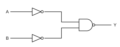
NEET 2023 · Q40 · Truth table of a given logic circuit
For the following logic circuit, the truth table is:
Logic circuit: A passes through a NOT gate and B through another NOT gate; the two outputs are the inputs of a NAND gate whose output is Y.
NTA's answer

Answer: (1) A B Y: 0 0 0; 0 1 1; 1 0 1; 1 1 1

From NTA's final answer key for NEET 2023.

NEET 2022

NEET 2022 · Q9 · Output frequency of a half wave rectifier
In half wave rectification, if the input frequency is 60 Hz, then the output frequency would be:
NTA's answer

Answer: (1) 60 Hz

From NTA's final answer key for NEET 2022.
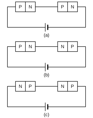
NEET 2022 · Q27 · Circuits in which two p-n junctions have equal potential drops
In the given circuits (a), (b) and (c), the potential drop across the two p-n junctions are equal in:
Three series circuits (a), (b), (c), each with two p-n junctions drawn as boxes on the top wire and a cell on the bottom wire, its long plate on the left: (a) P|N and P|N; (b) P|N and N|P; (c) N|P and N|P.
NTA's answer

Answer: (2) Both circuits (a) and (c)

From NTA's final answer key for NEET 2022.
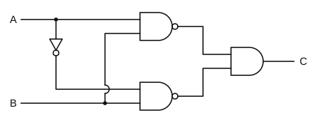
NEET 2022 · Q48 · Truth table of a given logic circuit
The truth table for the given logic circuit is:
Logic circuit: A goes to an upper NAND gate and, through a NOT gate, to a lower NAND gate; B goes to the lower NAND gate and to the upper NAND gate; the two NAND outputs feed an AND gate whose output is C. Options are truth tables with columns A, B, C.
NTA's answer

Answer: (1)

From NTA's final answer key for NEET 2022.

NEET 2021

NEET 2021 · Q2 · Statements on Zener diode biasing and p-n junction barrier potential
Consider the following statements (A) and (B) and identify the correct answer.
(A) A Zener diode is connected in reverse bias, when used as a voltage regulator.
(B) The potential barrier of p-n junction lies between 0.1 V to 0.3 V.
NTA's answer

Answer: (2) (A) is correct and (B) is incorrect.

From NTA's final answer key for NEET 2021.

NEET 2021 · Q17 · Currents in n-type and p-type semiconductors with equal carrier concentration
The electron concentration in an n-type semiconductor is the same as hole concentration in a p-type semiconductor. An external field (electric) is applied across each of them. Compare the currents in them.
NTA's answer

Answer: (2) Current in n-type > current in p-type

From NTA's final answer key for NEET 2021.
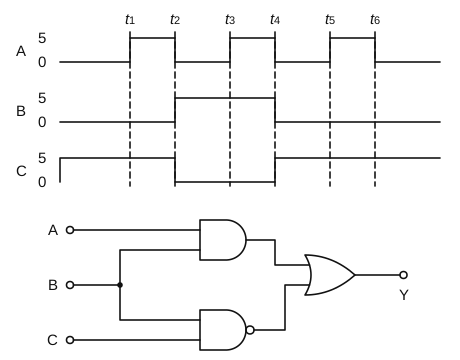
NEET 2021 · Q50 · Output waveform of a logic circuit for given digital inputs
For the given circuit, the input digital signals are applied at the terminals A, B and C. What would be the output at the terminal Y?
Input waveforms (levels 0 and 5) with instants t1 to t6 marked by dashed lines: A high from t1 to t2, t3 to t4 and t5 to t6; B high from t2 to t4; C high until t2 and again after t4. Circuit: A and B into an AND gate, B and C into a NAND gate, both outputs into an OR gate with output Y. Options: output Y against time on the same time scale: (1) a flat line at 0 with t1–t6 marked; (2) 0 V, then 5 V from t1 to t3, 0 V from t3 to t6, 5 V after t6; (3) a flat line at 5 V; (4) 5 V, then 0 V from t1 to t3, 5 V from t3 to t6, 0 V after t6.
NTA's answer

Answer: (3)

From NTA's final answer key for NEET 2021.

NEET 2020
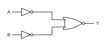
NEET 2020 · Q111 · Truth table of a logic circuit of NOT and NOR gates
For the logic circuit shown, the truth table is:
Input A goes through a NOT gate and input B through a second NOT gate; the two inverted signals are the inputs of a NOR gate (an OR shape with a bubble at its output), whose output is Y. Each option is a truth table with columns A, B, Y and rows 00, 01, 10, 11.
Answer

NTA's official answer key for NEET 2020 is not in hand yet. This page will carry the answer when it is; we do not put an answer of our own in its place.
NEET 2020 · Q117 · Cause of widening of the depletion region in a p-n junction
The increase in the width of the depletion region in a p-n junction diode is due to:
Answer

NTA's official answer key for NEET 2020 is not in hand yet. This page will carry the answer when it is; we do not put an answer of our own in its place.

NEET 2020 · Q134 · Condition for transistor action
For transistor action, which of the following statements is correct?
Answer

NTA's official answer key for NEET 2020 is not in hand yet. This page will carry the answer when it is; we do not put an answer of our own in its place.

NEET 2019 (Odisha)

NEET 2019 (Odisha) · Q3 · Wavelength of light emitted by an LED from its energy gap
An LED is constructed from a p-n junction diode using GaAsP. The energy gap is 1.9 eV. The wavelength of the light emitted will be equal to
Answer

NTA's official answer key for NEET 2019 (Odisha) is not in hand yet. This page will carry the answer when it is; we do not put an answer of our own in its place.

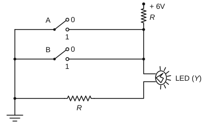
NEET 2019 (Odisha) · Q43 · Logic gate corresponding to a circuit diagram
The circuit diagram shown here corresponds to the logic gate,
A +6V terminal feeds a resistor R down to a vertical line on the right; two switches A (upper) and B (lower), each with an upper contact 0 and a contact 1 and shown at 0, have their pivots on a vertical line on the left that runs down to earth, and their contacts 1 wired to the right-hand line; the right-hand line continues to an LED labelled LED (Y), whose other lead returns through a second resistor R to the left earthed line.
Answer

NTA's official answer key for NEET 2019 (Odisha) is not in hand yet. This page will carry the answer when it is; we do not put an answer of our own in its place.

NEET 2019

NEET 2019 · Q15 · Charge carriers and dopant in a p-type semiconductor
For a p-type semiconductor, which of the following statements is true?
Answer

NTA's official answer key for NEET 2019 is not in hand yet. This page will carry the answer when it is; we do not put an answer of our own in its place.

NEET 2019 · Q44 · Boolean operation of a logic circuit

The correct Boolean operation represented by the circuit diagram drawn is:
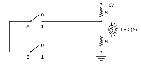
A vertical chain from a +6V terminal: resistor R, then an LED labelled LED (Y) with both leads on its left, then a second resistor R down to earth. Two switches A (upper) and B (lower), each with positions 0 and 1 and shown at 0, have their pivots joined by a wire on the left; switch A's contact 1 is wired to the point between the top R and the LED, and switch B's contact 1 to the earthed foot of the lower R.
Answer

NTA's official answer key for NEET 2019 is not in hand yet. This page will carry the answer when it is; we do not put an answer of our own in its place.
NEET 2018

NEET 2018 · Q9 · Effect of heating on a p-n junction diode
In a p-n junction diode, change in temperature due to heating
Answer

NTA's official answer key for NEET 2018 is not in hand yet. This page will carry the answer when it is; we do not put an answer of our own in its place.
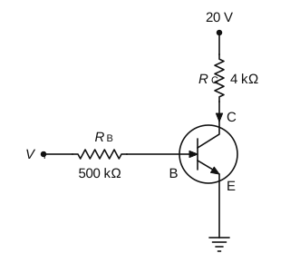
NEET 2018 · Q12 · Base current, collector current and gain of a transistor circuit
In the circuit shown in the figure, the input voltage Vi is 20 V, VBE = 0 and VCE = 0. The values of IB, IC and β are given by
An n-p-n transistor in common-emitter connection: the input Vi is joined through RB = 500 kΩ to the base B (arrow on the wire towards the base); the collector C is joined through RC = 4 kΩ to a terminal at 20 V; the emitter E, its arrow pointing out of the transistor, goes straight down to earth.
Answer

NTA's official answer key for NEET 2018 is not in hand yet. This page will carry the answer when it is; we do not put an answer of our own in its place.

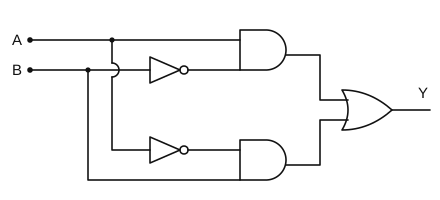
NEET 2018 · Q42 · Output of a combination of logic gates
In the combination of the following gates the output Y can be written in terms of inputs A and B as
Inputs A and B. A goes to the first input of an upper AND gate; B goes through a NOT gate to its second input. A also branches down (hopping over the B wire) through a second NOT gate to the first input of a lower AND gate; B branches down straight to the second input of the lower AND gate. The outputs of the two AND gates feed an OR gate whose output is Y.
Answer

NTA's official answer key for NEET 2018 is not in hand yet. This page will carry the answer when it is; we do not put an answer of our own in its place.

NEET 2017
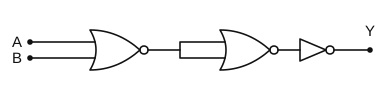
NEET 2017 · Q8 · Logic gate equivalent to a network of gates
The given electrical network is equivalent to
Inputs A and B feed a NOR gate; its output goes to both inputs of a second NOR gate (the two inputs joined); the second NOR's output goes through a NOT gate to the output Y.
Answer

NTA's official answer key for NEET 2017 is not in hand yet. This page will carry the answer when it is; we do not put an answer of our own in its place.

NEET 2017 · Q19 · Identifying a forward-biased diode
Which one of the following represents forward bias diode?
Answer

NTA's official answer key for NEET 2017 is not in hand yet. This page will carry the answer when it is; we do not put an answer of our own in its place.

NEET 2017 · Q43 · Voltage and power gain of a common-emitter amplifier
In a common emitter transistor amplifier, the audio signal voltage across the collector is 3 V. The resistance of collector is 3 kΩ. If current gain is 100 and the base resistance is 2 kΩ, the voltage and power gain of the amplifier is
Answer

NTA's official answer key for NEET 2017 is not in hand yet. This page will carry the answer when it is; we do not put an answer of our own in its place.

NEET 2016 Phase II
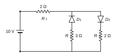
NEET 2016 Phase II · Q5 · Current in a circuit with two ideal diodes
The given circuit has two ideal diodes connected as shown in the figure below. The current flowing through the resistance R1 will be
A 10 V cell (long plate on top) on the left side of a circuit. From its top a wire runs through R1 = 2 Ω to a top rail; two branches hang from the top rail to the bottom rail: the first has diode D1 pointing up, towards the top rail, above R2 = 3 Ω; the second has diode D2 pointing down, away from the top rail, above R3 = 2 Ω. The bottom rail returns to the cell.
Answer

NTA's official answer key for NEET 2016 Phase II is not in hand yet. This page will carry the answer when it is; we do not put an answer of our own in its place.
NEET 2016 Phase II · Q11 · Input signal voltage of a common-emitter amplifier
For CE transistor amplifier, the audio signal voltage across the collector resistance of 2 kΩ is 4 V. If the current amplification factor of the transistor is 100 and the base resistance is 1 kΩ, then the input signal voltage is
Answer

NTA's official answer key for NEET 2016 Phase II is not in hand yet. This page will carry the answer when it is; we do not put an answer of our own in its place.

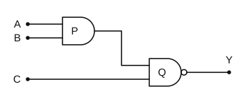
NEET 2016 Phase II · Q37 · Output of a logic circuit for given inputs
What is the output Y in the following circuit, when all the three inputs A, B, C are first 0 and then 1?
Inputs A and B feed an AND gate P; the output of P and input C feed a NAND gate Q (an AND shape with an output bubble), whose output is Y.
Answer

NTA's official answer key for NEET 2016 Phase II is not in hand yet. This page will carry the answer when it is; we do not put an answer of our own in its place.

NEET 2016 Phase I
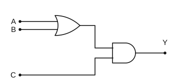
NEET 2016 Phase I · Q6 · Inputs giving output 1 for a logic circuit
To get an output 1 for the following circuit, the correct choice for the input is
Inputs A and B feed an OR gate; the OR gate's output and input C feed an AND gate, whose output is Y.
Answer

NTA's official answer key for NEET 2016 Phase I is not in hand yet. This page will carry the answer when it is; we do not put an answer of our own in its place.
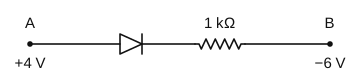
NEET 2016 Phase I · Q31 · Current through an ideal junction diode
Consider the junction diode as ideal. The value of current flowing through AB is
A line from point A, at +4 V, through a diode pointing from A towards B and then a 1 kΩ resistor, to point B, at −6 V.
Answer

NTA's official answer key for NEET 2016 Phase I is not in hand yet. This page will carry the answer when it is; we do not put an answer of our own in its place.

NEET 2016 Phase I · Q41 · Collector and base current of a common-emitter transistor amplifier
A npn transistor is connected in common emitter configuration in a given amplifier. A load resistance of 800 Ω is connected in the collector circuit and the voltage drop across it is 0.8 V. If the current amplification factor is 0.96 and the input resistance of the circuit is 192 Ω, the voltage gain and the power gain of the amplifier will respectively be
Answer

NTA's official answer key for NEET 2016 Phase I is not in hand yet. This page will carry the answer when it is; we do not put an answer of our own in its place.

AIPMT 2015 Re-Test
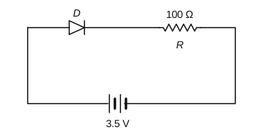
AIPMT 2015 Re-Test · Q4 · Current in a diode circuit with a barrier potential
In the given figure, a diode D is connected to an external resistance R = 100 Ω and an e.m.f of 3.5 V. If the barrier potential developed across the diode is 0.5 V, the current in the circuit will be
A series loop: along the top a diode D, pointing to the right, then a resistor R of 100 Ω; along the bottom a battery of two cells, 3.5 V, its long (positive) plates on the left.
Answer

NTA's official answer key for AIPMT 2015 Re-Test is not in hand yet. This page will carry the answer when it is; we do not put an answer of our own in its place.

AIPMT 2015 Re-Test · Q41 · Output signal of a common-emitter amplifier
The input signal given to a CE amplifier having a voltage gain of 150 is Vi = 2 cos (15t + π3). The corresponding output signal will be
Answer

NTA's official answer key for AIPMT 2015 Re-Test is not in hand yet. This page will carry the answer when it is; we do not put an answer of our own in its place.

AIPMT 2015

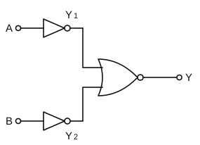
AIPMT 2015 · Q22 · Logic gate equivalent to a combination of gates
Which logic gate is represented by the following combination of logic gates?
Input A passes through a NOT gate, output Y₁; input B passes through a NOT gate, output Y₂. Y₁ and Y₂ are the two inputs of an OR gate with a bubble at its output (a NOR gate), whose output is Y.
Answer

NTA's official answer key for AIPMT 2015 is not in hand yet. This page will carry the answer when it is; we do not put an answer of our own in its place.

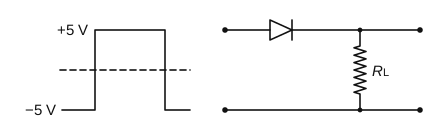
AIPMT 2015 · Q42 · Output of a p-n junction for a square input signal
If in a p-n junction, a square input signal of 10 V is applied, as shown

then the output across RL will be
Input: a square pulse between −5 V and +5 V with a dashed line marking zero midway; the signal is at −5 V, rises to +5 V, stays there and falls back to −5 V. Circuit: from the input terminals, a diode in series in the upper line pointing towards the output, and the load resistor R_L between the upper and lower lines, the output taken across it. Options, output waveforms: (1) a level line dropping to a pulse at −10 V and back; (2) a level line rising to a pulse at 10 V and back; (3) a level line dropping to a pulse at −5 V and back; (4) a level line rising to a pulse at 5 V and back.
Answer

NTA's official answer key for AIPMT 2015 is not in hand yet. This page will carry the answer when it is; we do not put an answer of our own in its place.

AIPMT 2014

AIPMT 2014 · Q1 · Factors that set the barrier potential of a p-n junction
The barrier potential of a p-n junction depends on:
a. Type of semiconductor material
b. Amount of doping
c. Temperature
Which one of the following is correct?
Answer

NTA's official answer key for AIPMT 2014 is not in hand yet. This page will carry the answer when it is; we do not put an answer of our own in its place.

AIPMT 2014 · Q40 · Identifying a device from its V-I characteristic
The given graph represents V – I characteristic for a semiconductor device.

Which of the following statements is correct?
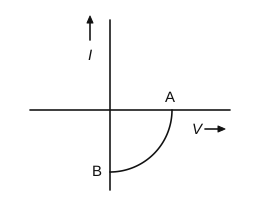
Axes I (vertical) and V (horizontal) crossing at the centre; a curve in the fourth quadrant bows outward from point A on the positive V axis to point B on the negative I axis.
Answer

NTA's official answer key for AIPMT 2014 is not in hand yet. This page will carry the answer when it is; we do not put an answer of our own in its place.

Free NEET chapter practice and testsSee the Class 12 flashcards

← Nuclei